Two-port network
A two-port network (a kind of four-terminal network or quadripole) is an electrical circuit or device with two pairs of terminals connected internally by an electrical network. Two terminals constitute a port if they satisfy the essential requirement known as the port condition: the same current must enter and leave a port.[1][2]
Examples include small-signal models for transistors (such as the hybrid-pi model), filters and matching networks. The analysis of passive two-port networks is an outgrowth of reciprocity theorems first derived by Lorentz.[3]
A two-port network makes possible the isolation of either a complete circuit or part of it and replacing it by its characteristic parameters. Once this is done, the isolated part of the circuit becomes a "black box" with a set of distinctive properties, enabling us to abstract away its specific physical buildup, thus simplifying analysis. Any linear circuit with four terminals can be transformed into a two-port network provided that it does not contain an independent source and satisfies the port conditions.
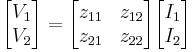
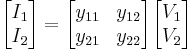
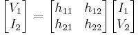
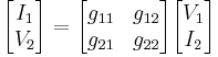
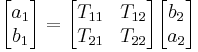
There are a number of alternative sets of parameters that can be used to describe a linear two-port network, the usual sets are respectively called z, y, h, g, and ABCD parameters, each described individually below. These are all limited to linear networks since an underlying assumption of their derivation is that any given circuit condition is a linear superposition of various short-circuit and open circuit conditions. They are usually expressed in matrix notation, and they establish relations between the variables
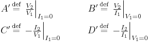
 Input voltage
 Output voltage
 Input current
 Output current
which are shown in Figure 1. These current and voltage variables are most useful at low-to-moderate frequencies. At high frequencies (e.g., microwave frequencies), the use of power and energy variables is more appropriate, and the two-port current–voltage approach is replaced by an approach based upon scattering parameters.
The terms four-terminal network and quadripole (not to be confused with quadrupole) are also used, the latter particularly in more mathematical treatments although the term is becoming archaic. However, a pair of terminals can be called a port only if the current entering one terminal is equal to the current leaving the other; this definition is called the port condition. A four-terminal network can only be properly called a two-port when the terminals are connected to the external circuitry in two pairs both meeting the port condition.[1][2]
General properties
There are certain properties of two-ports that frequently occur in practical networks and can be used to greatly simplify the analysis. These include:
Reciprocal networks. A network is said to be reciprocal if the voltage appearing at port 2 due to a current applied at port 1 is the same as the voltage appearing at port 1 when the same current is applied to port 2. Exchanging voltage and current results in an equivalent definition of reciprocity. In general, a network will be reciprocal if it consists entirely of linear passive components (that is, resistors, capacitors and inductors). In general, it will not be reciprocal if it contains active components such as generators.[4]
Symmetrical networks. A network is symmetrical if its input impedance is equal to its output impedance. Most often, but not necessarily, symmetrical networks are also physically symmetrical. Sometimes also antimetrical networks are of interest. These are networks where the input and output impedances are the duals of each other.[5]
Lossless network. A lossless network is one which contains no resistors or other dissipative elements.[6]
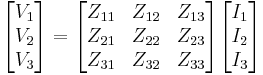
Impedance parameters (z-parameters)
where
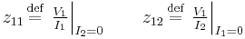
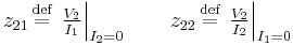
Notice that all the z-parameters have dimensions of ohms.
For reciprocal networks  . For symmetrical networks
  . For lossless networks all the
  are purely imaginary.[7]
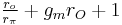
Example: bipolar current mirror with emitter degeneration
Figure 3 shows a bipolar current mirror with emitter resistors to increase its output resistance.[nb 1] Transistor Q1 is diode connected, which is to say its collector-base voltage is zero. Figure 4 shows the small-signal circuit equivalent to Figure 3. Transistor Q1 is represented by its emitter resistance rE ≈ VT / IE (VT = thermal voltage, IE = Q-point emitter current), a simplification made possible because the dependent current source in the hybrid-pi model for Q1 draws the same current as a resistor 1 / gm connected across rπ. The second transistor Q2 is represented by its hybrid-pi model. Table 1 below shows the z-parameter expressions that make the z-equivalent circuit of Figure 2 electrically equivalent to the small-signal circuit of Figure 4.
| Table 1 | Expression | Approximation |
|---|---|---|
 |
 |
 |
 |
 |
|
 |
 |
 |
 |
  |
 |
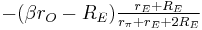
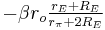
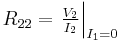
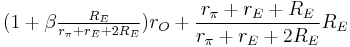
The negative feedback introduced by resistors RE can be seen in these parameters. For example, when used as an active load in a differential amplifier, I1 ≈ -I2, making the output impedance of the mirror approximately R22 -R21 ≈ 2 β rORE /( rπ+2RE ) compared to only rO without feedback (that is with RE = 0 Ω) . At the same time, the impedance on the reference side of the mirror is approximately R11 − R12 ≈ 
 , only a moderate value, but still larger than rE with no feedback. In the differential amplifier application, a large output resistance increases the difference-mode gain, a good thing, and a small mirror input resistance is desirable to avoid Miller effect.
Admittance parameters (y-parameters)
where
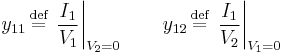
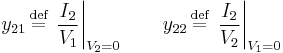
Notice that all the Y-parameters have dimensions of siemens.
For reciprocal networks  . For symmetrical networks
  . For lossless networks all the
  are purely imaginary.[7]
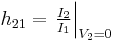
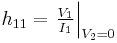
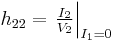
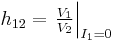
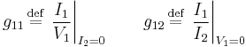
Hybrid parameters (h-parameters)
where
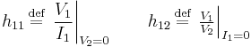
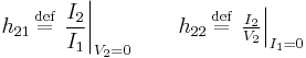
This circuit is often selected when a current amplifier is wanted at the output. The resistors shown in the diagram can be general impedances instead.
Notice that off-diagonal h-parameters are dimensionless, while diagonal members have dimensions the reciprocal of one another.
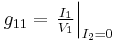
Example: common-base amplifier
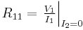
Note: Tabulated formulas in Table 2 make the h-equivalent circuit of the transistor from Figure 6 agree with its small-signal low-frequency hybrid-pi model in Figure 7. Notation: rπ = base resistance of transistor, rO = output resistance, and gm = transconductance. The negative sign for h21 reflects the convention that I1, I2 are positive when directed into the two-port. A non-zero value for h12 means the output voltage affects the input voltage, that is, this amplifier is bilateral. If h12 = 0, the amplifier is unilateral.
| Table 2 | Expression | Approximation |
|---|---|---|
 |
 |
 |
 |
 |
 |
 |
 |
 |
 |
 |
 |
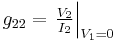
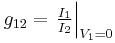
Inverse hybrid parameters (g-parameters)
where
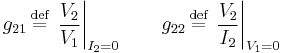
Often this circuit is selected when a voltage amplifier is wanted at the output. Notice that off-diagonal g-parameters are dimensionless, while diagonal members have dimensions the reciprocal of one another. The resistors shown in the diagram can be general impedances instead.
Example: common-base amplifier
Note: Tabulated formulas in Table 3 make the g-equivalent circuit of the transistor from Figure 8 agree with its small-signal low-frequency hybrid-pi model in Figure 9. Notation: rπ = base resistance of transistor, rO = output resistance, and gm = transconductance. The negative sign for g12 reflects the convention that I1, I2 are positive when directed into the two-port. A non-zero value for g12 means the output current affects the input current, that is, this amplifier is bilateral. If g12 = 0, the amplifier is unilateral.
| Table 3 | Expression | Approximation |
|---|---|---|
 |
 |
 |
 |
 |
|
 |
 |
|
 |
 |
 |
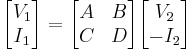
ABCD-parameters
The ABCD-parameters are known variously as chain, cascade, or transmission line parameters. There are a number of definitions given for ABCD parameters, the most common is,[8][9]
For reciprocal networks  . For symmetrical networks
  . For networks which are reciprocal and lossless, A and D are purely real while B and C are purely imaginary.[6]
This representation is preferred because when the parameters are used to represent a cascade of two-ports, the matrices are written in the same order that a network diagram would be drawn, that is, left to right. However, the examples given below are based on a variant definition;
where
The negative signs in the definitions of parameters  and
and  arise because
  is defined with the opposite sense to
  , that is,
  . The reason for adopting this convention is so that the output current of one cascaded stage is equal to the input current of the next. Consequently, the input voltage/current matrix vector can be directly replaced with the matrix equation of the preceding cascaded stage to form a combined
  matrix.
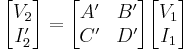
The terminology of representing the  parameters as a matrix of elements designated a11 etc. as adopted by some authors[10] and the inverse parameters as a matrix of elements designated b11 etc. is used here for both brevity and to avoid confusion with circuit elements.
![[\mathbf a]= \begin{bmatrix} a_{11} & a_{12} \\ a_{21} & a_{22} \end{bmatrix} = \begin{bmatrix} A & B \\ C & D \end{bmatrix}](/2012-wikipedia_en_all_nopic_01_2012/I/9c4589dad051ea512b263bd010de17f7.png)
![[\mathbf b]= \begin{bmatrix} b_{11} & b_{12} \\ b_{21} & b_{22} \end{bmatrix} = \begin{bmatrix} A' & B' \\ C' & D' \end{bmatrix}](/2012-wikipedia_en_all_nopic_01_2012/I/a0518f177fecafa3fee6db9f09f791c2.png)
There is a simple relationship between these two forms: one is the matrix inverse of the other, that is;
![[\mathbf b]=[\mathbf a]^{-1}](/2012-wikipedia_en_all_nopic_01_2012/I/2a14493372a7f9530559c6a2d8e2ccd1.png)
An ABCD matrix has been defined for Telephony four-wire Transmission Systems by P K Webb in British Post Office Research Department Report 630 in 1977.
Table of transmission parameters
The table below lists inverse ABCD parameters for some simple network elements.
| Element | [b] matrix | Remarks |
|---|---|---|
| Series resistor |  |
R = resistance |
| Shunt resistor | 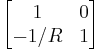 |
R = resistance |
| Series conductor | 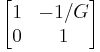 |
G = conductance |
| Shunt conductor |  |
G = conductance |
| Series inductor |  |
L = inductance s = complex angular frequency |
| Shunt capacitor |  |
C = capacitance s = complex angular frequency |
Combinations of two-port networks
When two or more two-port networks are connected, the two-port parameters of the combined network can be found by performing matrix algebra on the matrices of parameters for the component two-ports. The matrix operation can be made particularly simple with an appropriate choice of two-port parameters to match the form of connection of the two-ports. For instance, the z-parameters are best for series connected ports.
The combination rules need to be applied with care. Some connections (when dissimilar potentials are joined) result in the port condition being invalidated and the combination rule will no longer apply. This difficulty can be overcome by placing 1:1 ideal transformers on the outputs of the problem two-ports. This does not change the parameters of the two-ports, but does ensure that they will continue to meet the port condition when interconnected. An example of this problem is shown for series-series connections in figures 11 and 12 below.[11]
Series-series connection
When two-ports are connected in a series-series configuration as shown in figure 10, the best choice of two-port parameter is the z-parameters. The z-parameters of the combined network are found by matrix addition of the two individual z-parameter matrices.[12][13]
![[\mathbf z]=[\mathbf z]_1 %2B [\mathbf z]_2](/2012-wikipedia_en_all_nopic_01_2012/I/1127d18858a91c76edcc86366eaa377e.png)
As mentioned above, there are some networks which will not yield directly to this analysis.[11] A simple example is a two-port consisting of a L-network of resistors R1 and R2. The z-parameters for this network are;
![[\mathbf z]_1 = \begin{bmatrix} R_1 %2B R_2 & R_2 \\ R_2 & R_2 \end{bmatrix}](/2012-wikipedia_en_all_nopic_01_2012/I/dd72055e7db3087952e48ba0edb988cc.png)
Figure 11 shows two identical such networks connected in series-series. The total z-parameters predicted by matrix addition are;
![[\mathbf z] =[\mathbf z]_1 %2B [\mathbf z]_2 = 2[\mathbf z]_1 = \begin{bmatrix} 2R_1 %2B 2R_2 & 2R_2 \\ 2R_2 & 2R_2 \end{bmatrix}](/2012-wikipedia_en_all_nopic_01_2012/I/7ad1f7a8c7bbc92dbb8e88890c376c18.png)
However, direct analysis of the combined circuit shows that,
![[\mathbf z] = \begin{bmatrix} R_1 %2B 2R_2 & 2R_2 \\ 2R_2 & 2R_2 \end{bmatrix}](/2012-wikipedia_en_all_nopic_01_2012/I/1c43d3f1181009a128b8b85431969b80.png)
The discrepancy is explained by observing that R1 of the lower two-port has been by-passed by the short-circuit between two terminals of the output ports. This results in no current flowing through one terminal in each of the input ports of the two individual networks. Consequently, the port condition is broken for both the input ports of the original networks since current is still able to flow into the other terminal. This problem can be resolved by inserting an ideal transformer in the output port of at least one of the two-port networks. While this is a common text-book approach to presenting the theory of two-ports, the practicality of using transformers is a matter to be decided for each individual design.
Parallel-parallel connection
When two-ports are connected in a parallel-parallel configuration as shown in figure 13, the best choice of two-port parameter is the y-parameters. The y-parameters of the combined network are found by matrix addition of the two individual y-parameter matrices.[14]
![[\mathbf y]=[\mathbf y]_1 %2B [\mathbf y]_2](/2012-wikipedia_en_all_nopic_01_2012/I/004e1d818d8305214391531679e3f6b4.png)
Series-parallel connection
When two-ports are connected in a series-parallel configuration as shown in figure 14, the best choice of two-port parameter is the h-parameters. The h-parameters of the combined network are found by matrix addition of the two individual h-parameter matrices.[15]
![[\mathbf h]=[\mathbf h]_1 %2B [\mathbf h]_2](/2012-wikipedia_en_all_nopic_01_2012/I/a393d4bb63142fdc889d0c2e415b3581.png)
Parallel-series connection
When two-ports are connected in a parallel-series configuration as shown in figure 15, the best choice of two-port parameter is the g-parameters. The g-parameters of the combined network are found by matrix addition of the two individual g-parameter matrices.
![[\mathbf g]=[\mathbf g]_1 %2B [\mathbf g]_2](/2012-wikipedia_en_all_nopic_01_2012/I/5c79c7bb418bb408456aaf45205fb721.png)
Cascade connection
When two-ports are connected with the output port of the first connected to the input port of the second (a cascade connection) as shown in figure 16, the best choice of two-port parameter is the ABCD-parameters. The a-parameters of the combined network are found by matrix multiplication of the two individual a-parameter matrices.[16]
![[\mathbf a]=[\mathbf a]_1 \cdot [\mathbf a]_2](/2012-wikipedia_en_all_nopic_01_2012/I/077fa8512d01033f920e5c0aeee4812f.png)
A chain of n two-ports may be combined by matrix multiplication of the n matrices. To combine a cascade of b-parameter matrices, they are again multiplied, but the multiplication must be carried out in reverse order, so that;
![[\mathbf b]=[\mathbf b]_2 \cdot [\mathbf b]_1](/2012-wikipedia_en_all_nopic_01_2012/I/180cbf40599dd56ddd5e245b12aedc4f.png)
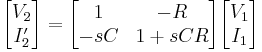
Example
Suppose we have a two-port network consisting of a series resistor R followed by a shunt capacitor C. We can model the entire network as a cascade of two simpler networks:
![[\mathbf b]_1 = \begin{bmatrix} 1 & -R \\ 0 & 1 \end{bmatrix}](/2012-wikipedia_en_all_nopic_01_2012/I/8af8fddcea44569edd23fe467077100a.png)
![[\mathbf b]_2 = \begin{bmatrix} 1 & 0 \\ -sC & 1 \end{bmatrix}](/2012-wikipedia_en_all_nopic_01_2012/I/7a689dc63e3a8766cc3bce843ffdc0c9.png)
The transmission matrix for the entire network ![\scriptstyle [\mathbf b]](/2012-wikipedia_en_all_nopic_01_2012/I/23585f0c3d2165a9fbc3cc0fe715cc9e.png) is simply the matrix multiplication of the transmission matrices for the two network elements:
is simply the matrix multiplication of the transmission matrices for the two network elements:
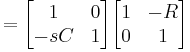
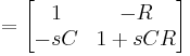
Thus:
Scattering parameters (S-parameters)
The previous parameters are all defined in terms of voltages and currents at ports. S-parameters are different, and are defined in terms of incident and reflected waves at ports. S-parameters are used primarily at UHF and microwave frequencies where it becomes difficult to measure voltages and currents directly. On the other hand, incident and reflected power are easy to measure using directional couplers. The definition is,[17]
where the  are the incident waves and the
  are the reflected waves at port k. It is conventional to define the and in terms of the square root of power. Consequently, there is a relationship with the wave voltages (see main article for details).[18]
For reciprocal networks  . For symmetrical networks
  . For antimetrical networks
  .[19] For lossless reciprocal networks
  and
and  .[20]
.[20]
Scattering transfer parameters (T-parameters)
Scattering transfer parameters, like scattering parameters, are defined in terms of incident and reflected waves. The difference is that T-parameters relate the waves at port 1 to the waves at port 2 whereas S-parameters relate the reflected waves to the incident waves. In this respect T-parameters fill the same role as ABCD parameters and allow the T-parameters of cascaded networks to be calculated by matrix multiplication of the component networks. T-parameters, like ABCD parameters, can also be called transmission parameters. The definition is,[17][21]
T-parameters are not so easy to measure directly unlike S-parameters. However, S-parameters are easily converted to T-parameters, see main article for details.[22]
Networks with more than two ports
While two port networks are very common (e.g. amplifiers and filters), other electrical networks such as directional couplers and circulators have more than 2 ports. The following representations are also applicable to networks with an arbitrary number of ports:
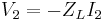
For example three-port impedance parameters result in the following relationship:
However the following representations are necessarily limited to two-port devices:
- Hybrid (h) parameters
- Inverse hybrid (g) parameters
- Transmission (ABCD) parameters
- Scattering transfer (T) parameters
Collapsing a two-port to a one port
A two-port network has four variables with two of them being independent. If one of the ports is terminated by a load with no independent sources, then the load enforces a relationship between the voltage and current of that port. A degree of freedom is lost. The circuit now has only one independent parameter. The two-port becomes a one-port impedance to the remaining independent variable.
For example, consider impedance parameters
Connecting a load, ZL onto port 2 effectively adds the constraint
The negative sign is because the positive direction for I2 is directed into the two-port instead of into the load. The augmented equations become
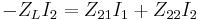
The second equation can be easily solved for I2 as a function of I1 and that expression can replace I2 in the first equation leaving V1 ( and V2 and I2 ) as functions of I1
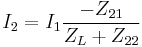

So, in effect, I1 sees an input impedance  and the two-port's effect on the input circuit has been effectively collapsed down to a one-port i.e. a simple two terminal impedance.
See also
Notes
- ^ The emitter-leg resistors counteract any current increase by decreasing the transistor VBE. That is, the resistors RE cause negative feedback that opposes change in current. In particular, any change in output voltage results in less change in current than without this feedback, which means the output resistance of the mirror has increased.
References
- ^ a b Gray, §3.2, p. 172
- ^ a b Jaeger, §10.5 §13.5 §13.8
- ^ Jasper J. Goedbloed, Reciprocity and EMC measurements
- ^ Nahvi, p.311.
- ^ Matthaei et al, pp. 70–72.
- ^ a b Matthaei et al, p.27.
- ^ a b Matthaei et al, p.29.
- ^ Matthaei et al, p.26.
- ^ Ghosh, p.353.
- ^ Farago, p.102.
- ^ a b Farago, pp.122-127.
- ^ Ghosh, p.371.
- ^ Farago, p.128.
- ^ Ghosh, p.372.
- ^ Ghosh, p.373.
- ^ Farago, pp.128-134.
- ^ a b Vasileska & Goodnick, p.137
- ^ Egan, pp.11-12
- ^ Carlin, p.304
- ^ Matthaei et al, p.44.
- ^ Egan, pp.12-15
- ^ Egan, pp.13-14
Bibliography
- Carlin, HJ, Civalleri, PP, Wideband circuit design, CRC Press, 1998. ISBN 0849378974.
- William F. Egan, Practical RF system design, Wiley-IEEE, 2003 ISBN 0471200239.
- Farago, PS, An Introduction to Linear Network Analysis, The English Universities Press Ltd, 1961.
- Gray, P.R.; Hurst, P.J.; Lewis, S.H.; Meyer, R.G. (2001). Analysis and Design of Analog Integrated Circuits (4th ed.). New York: Wiley. ISBN 0471321680.
- Ghosh, Smarajit, Network Theory: Analysis and Synthesis, Prentice Hall of India ISBN 8120326385.
- Jaeger, R.C.; Blalock, T.N. (2006). Microelectronic Circuit Design (3rd ed.). Boston: McGraw–Hill. ISBN 9780073191638.
- Matthaei, Young, Jones, Microwave Filters, Impedance-Matching Networks, and Coupling Structures, McGraw-Hill, 1964.
- Mahmood Nahvi, Joseph Edminister, Schaum's outline of theory and problems of electric circuits, McGraw-Hill Professional, 2002 ISBN 0071393072.
- Dragica Vasileska, Stephen Marshall Goodnick, Computational electronics, Morgan & Claypool Publishers, 2006 ISBN 1598290568.